Control Connector#
25-pin sub-D#
Supported devices: [MH150/160 | PH330]
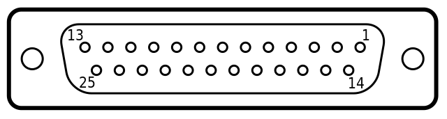
The control connector is a 25-pin female sub-D connector labeled CTRL.
The following figure shows the pin layout and the table below contains the connector’s default pin assignments.
Pin # |
Name |
I/O |
Purpose/Description |
|---|---|---|---|
1 |
GPIO 0 |
TTL in |
marker 1 input |
2 |
GPIO 1 |
TTL in |
marker 2 input |
3 |
GPIO 2 |
TTL in |
marker 3 input |
4 |
GPIO 3 |
TTL in |
marker 4 input |
5 |
GPIO 4 |
TTL in |
reserved |
6 |
GPIO 5 |
TTL in |
reserved |
7 |
GPIO 6 |
TTL in |
reserved |
8 |
GPIO 7 |
TTL in |
reserved |
9 |
GPIO 8 |
TTL in |
reserved |
10 |
GPIO 9 |
TTL in |
reserved |
11 |
GPIO 10 |
TTL in |
reserved |
12 |
GPIO 11 |
TTL in |
reserved |
13 |
GPIO 12 |
TTL in |
reserved |
14 |
GND |
GND |
reserved |
15 |
GPIO 13 |
TTL in |
reserved |
16 |
GPIO 14 |
TTL in |
ground (0V) |
17 |
GPIO 15 |
TTL in |
RS232 RX (3.3V signal level) for connection to GPS/GLONASS receiver |
18 |
GND |
GND |
ground (0V) |
19 |
C1 |
TTL in |
start measurement |
20 |
C2 |
TTL in |
stop measurement |
21 |
GND |
GND |
ground (0V) |
22 |
MACT |
TTL out |
high when measurement running |
23 |
GND |
TTL in |
ground (0V) |
24 |
D3V3 |
DC out |
+3.3V / ≤ 350 mA supply for external hardware add-ons |
25 |
GND |
GND |
ground (0V) |
Note
A maximum high level of 3.3V is permitted.
Marker#
Pin 1, 2, 3 and 4 accept TTL compatible synchronization signals that will be recorded as markers in T2/T3
mode. The pins are internally pulled down, so that they are inactive when left unconnected. The active edge
can be set with Device.setMarkerEdges and is at least 50 ns long.
The clock period may therefore (in principle) be as short as about 100 ns but data bus throughput constraints will apply.
Each marker creates an additional data record, so that one must ensure not to swamp the data stream with too many marker records.
When bandwidth gets tight, markers take precedence over photon records, so that excess marker traffic can
suppress photon records. In fast imaging applications it is therefore recommended not to use a pixel clock
but a line clock only. Because each photon has a time tag, it is usually not necessary to use an additional
pixel clock.
External Clock#
Pin 17 can be used to connect the serial TX line of a GPS/GLONASS receiver for time transmission via the
NMEA ZDA Message protocol at 115.2 kbps, 3.3V. We have successfully tested this with the Mini-T™ GG disciplined
clock module from Trimble Inc., USA.
Set snAPI.Constants.RefSource to RefSource.Extn_GPS_PPS in snAPI.initDevice.
Hardware triggered measurements#
Pins 19 and 20 can be used to implement hardware triggered measurements. Therefore ou have to set Device.setMeasControl
to MeasControl.C1Gated, MeasControl.C1StartCtcStop or MeasControl.C1StartC2Stop.
- See:
Additional Features#
Pin 22 is a TTL output that goes high when a measurement is running. Pin 24 provides a 3.3 V DC supply voltage that external electronics can use. Under no circumstances must this line be shorted to ground or loaded in excess of the specified maximum current. Pin 14, 18, 21, 23, and 25 are the common ground for the TTL signals and the DC supply line. They are also connected to the housing.
Note
Appropriate cables for typical applications of the control port are available from PicoQuant.
15-pin sub-D#
Supported devices: [TH260]
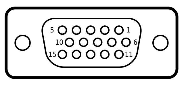
The control connector is a 15-pin female sub-D connector located on the slot bracket and labelled C.
The following table shows the control connector’s pin assignments
Pin # |
I/O |
Purpose/Description |
|---|---|---|
1 |
TTL out |
debug output - do not connect! |
2 |
TTL in |
disable sync channel (T2 mode only) |
3 |
TTL out |
high when measurement running |
4 |
TTL in |
marker 2 input |
5 |
TTL in |
marker 3 input |
6 |
TTL in |
disable input channel 1 |
7 |
NIM out |
trigger out (programmable rate) |
8 |
TTL in |
disable input channel 2 |
9 |
TTL in |
marker 1 input |
10 |
TTL in |
marker 4 input |
11 |
DC out |
|
12 |
GND |
ground (0V) |
13 |
TTL in |
C1 Start measurement |
14 |
GND |
ground (0V) |
15 |
GND |
C2 Stop measurement |
Channel Disabling#
Pin 2, 6, and 8 accept the TTL compatible signals to disable event recording on individual channels. By default, when the respective pin is unconnected, recording is enabled. When the pin is driven by external logic then the enabled state is TTL low and the disabled state is TTL high. Note that the sync channel can only be disabled in T2 mode. Also note that this kind of enabling is not designed for precise timing in the sense of temporal gating. The temporal precision is only on the order on some tens of nanoseconds and disabling the channel does not prevent dead time.
Markers#
Pin 4, 5, 9 and 10 accept the TTL compatible synchronization signals that will be recorded as markers in
TTTR mode. Note that this requires a DUAL model, markers are not supported in the SINGLE models. The
pins are internally pulled down, so that they are inactive when left unconnected. The active edge
can be set with Device.setMarkerEdges.
Rise/fall times must be 10 ns or faster. Both high and low state must be at least 50 ns long. The clock
period may therefore (in principle) be as short as 100 ns but data bus throughput constraints
will apply. Each marker creates an additional TTTR record, so that one must ensure not to swamp the
data stream with too many marker records. When bandwidth gets tight, markers take precedence over photon
records, so that excess marker traffic can suppress photon records. In fast imaging applications it is therefore
recommended not to use a pixel clock but a line clock only. Because each photon has a time tag, it is usually
not necessary to use an additional pixel clock.
Hardware triggered measurements#
Pin 13 and 15 can be used to implement hardware triggered measurements. Therefore ou have to set Device.setMeasControl
to MeasControl.C1Gated, MeasControl.C1StartCtcStop or MeasControl.C1StartC2Stop.
See
Additional Features#
Pin 7 provides a programmable trigger output for light sources. Trigger out is only available with TH260N or with TH260P
in Device.setTimingMode set to 1 (long range mode).
Pin 11 provides a 5 V DC supply voltage external electronics can use. Under no circumstances must this line
be shorted or loaded in excess of the specified maximum current.
Pin 12 and 14 are the common ground for the TTL signals and the DC supply line. They are also connected to
the PC chassis.